Sr Flip Flop Timing Diagram, D Flip Flop Or D Latch What Is It Truth Table Timing Diagram Electrical4u
- Digital Teaching Aid Flip Flops Lesson 7 Lesson Plan Rs Flip Flops
- Diy Clocked Sr Flip Flop
- Homework 5 With Solutions Homework Eecs 31 Cse 31 Ics 151 Daniel D Gajski S Web Site
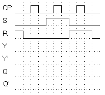
- Sr Flip Flops
- Sr Latch Timing Diagram Youtube
- Pengertian Dan Macam Macam Rangkaian Flip Flop Katakoala
- Dee2034 Chapter 4 Flip Flop For Students Part
- Flip Flop Circuits
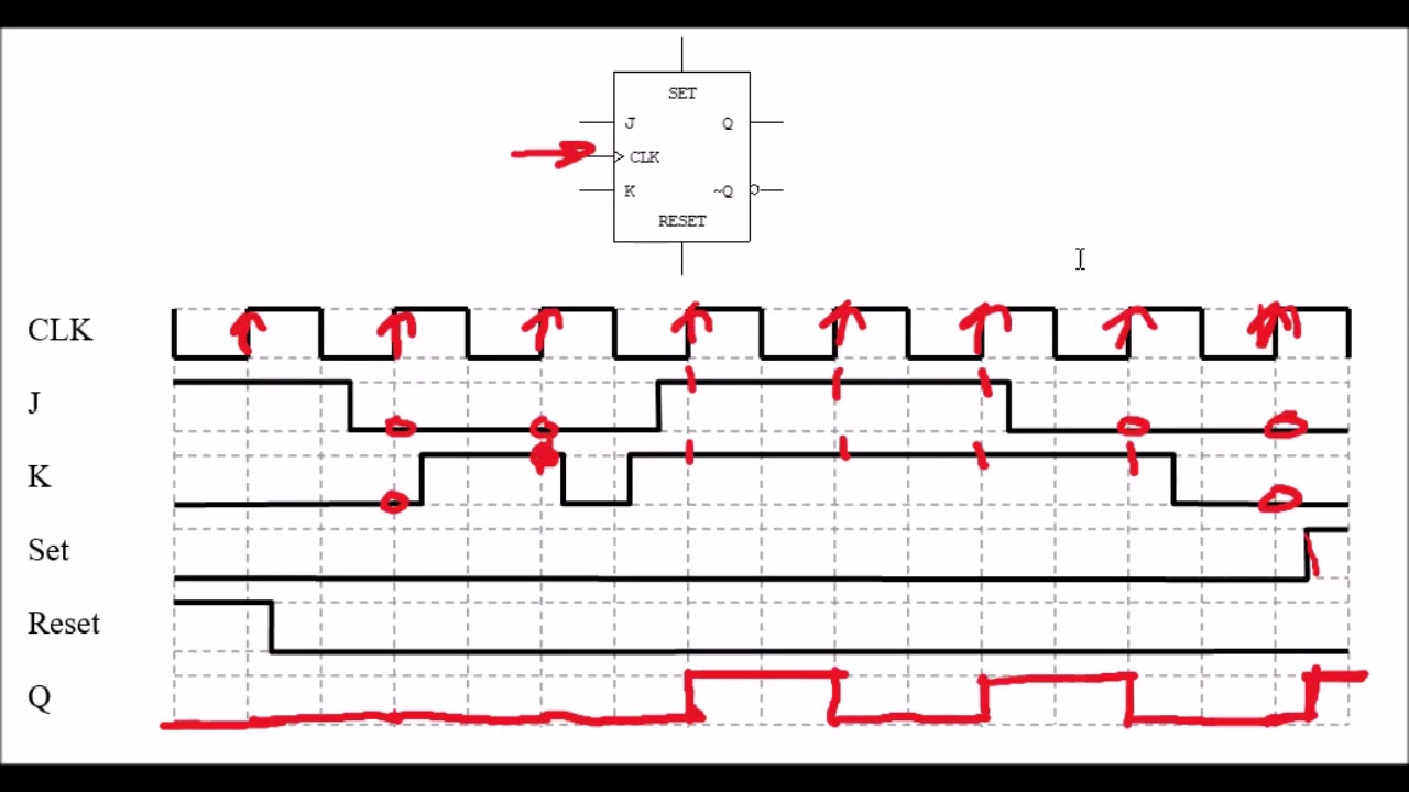
- Master Slave Jk Flip Flop Geeksforgeeks
- Digital Circuits Flip Flops Tutorialspoint
Find, Read, And Discover Sr Flip Flop Timing Diagram, Such Us:
- Sr Flip Flop Sequential Logic Circuits Electronics Tutorial
- Jk Flip Flop D Flip Flop Using Sr Flip Flop
- Conversion Of Sr Flip Flop To T Flip Flop Electronics Engineering Study Center
- Symmetrical And Non Symmetrical Flip Flop Diagrams Download Scientific Diagram
- Sr Flip Flop Circuit Diagram With Nand Gates Working Truth Table Explained
If you are searching for Boost Converter Diagram you've reached the ideal place. We ve got 104 images about boost converter diagram adding pictures, photos, pictures, wallpapers, and much more. In these web page, we also have number of graphics available. Such as png, jpg, animated gifs, pic art, symbol, black and white, transparent, etc.
Flip Flops Boost Converter Diagram
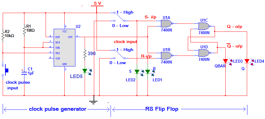
Diy Clocked Sr Flip Flop Boost Converter Diagram

Pengertian Dan Macam Macam Rangkaian Flip Flop Katakoala Boost Converter Diagram
Jk Flip Flop Timing Diagrams Youtube Boost Converter Diagram
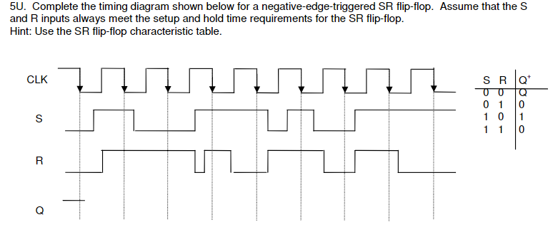
Solved 5u Complete The Timing Diagram Shown Below For A Chegg Com Boost Converter Diagram
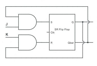
Jk Flip Flop D Flip Flop Using Sr Flip Flop Boost Converter Diagram

The Jk Flip Flop Boost Converter Diagram
Edge Triggered Latches Flip Flops Instrumentationtools Boost Converter Diagram
Sr Flip Flop Circuit Diagram With Nand Gates Working Truth Table Explained Boost Converter Diagram
Sr Latch Timing Diagram Youtube Boost Converter Diagram
Boost Converter Diagram, Ppt Chapter5 Synchronous Sequential Logic Part 1 Powerpoint Presentation Id 3630283
- Pengertian Dan Macam Macam Rangkaian Flip Flop Katakoala
- Latch Vs Flip Flop Difference Between Latch And Flip Flop
- Solved Given A Positive Edge Triggered Sr Flip Flop Comp Chegg Com
Boost Converter Diagram, Flip Flops Basic Concepts 1 50a Yaicharoen2 Flip Flops A Flip Flop Is A Bi Stable Device A Circuit Having 2 Stable Conditions 0 Or 1 3 Classes Of Ppt Download
- Sequential Circuits Tutorialspoint
- Digital Logic Part 2 Flip Flopsrheingold Heavy
- Flip Flops Digital Circuits 4 Sequential Circuits Adafruit Learning System
Boost Converter Diagram, Flip Flop Electronics Wikipedia
- Http Elektro Um Ac Id Wp Content Uploads 2016 04 Elektronika Digital Dasar Modul 9 Flip Flop S R Pdf
- Latch Vs Flip Flop Combinational Circuits In The Digital By Jay Mistry Medium
- S R Flip Flop Computer Organization And Architecture Tutorial Javatpoint
More From Boost Converter Diagram
- Bohr Rutherford Diagram Of Hydrogen
- Diagram Of D Heart
- Bit3260 Circuit Diagram
- Lutron 3 Way Switch Diagram
- Cell Diagram Labeled Human
Incoming Search Terms:
- Latch Vs Flip Flop Difference Between Latch And Flip Flop Cell Diagram Labeled Human,
- Jk Flip Flop What Is It Truth Table Timing Diagram Electrical4u Cell Diagram Labeled Human,
- Sr Latch Timing Diagram Youtube Cell Diagram Labeled Human,
- Jk Flip Flop Power Electronic Cell Diagram Labeled Human,
- Sr Flip Flop Diagram Truth Table Excitation Table Gate Vidyalay Cell Diagram Labeled Human,
- Sr Latch Timing Diagram Or Waveform With Delay Help Electrical Engineering Stack Exchange Cell Diagram Labeled Human,