Pmos Circuit Diagram, Mosfet And Metal Oxide Semiconductor Tutorial
- Http Tuttle Merc Iastate Edu Ee230 Topics Mosfets Pmos Pdf
- Https Encrypted Tbn0 Gstatic Com Images Q Tbn And9gct41pqmv5g48gtvzxrqpvottegkwohy2thxo9jdo63wj9ya8c2i Usqp Cau
- Pmos Fet Following The Output For Soft Start Mechanism Simple Circuit Diagram
- Pmos Nor Gate Youtube
- Lab
- Pmos 1 1 Multisim Live
- Lab 7
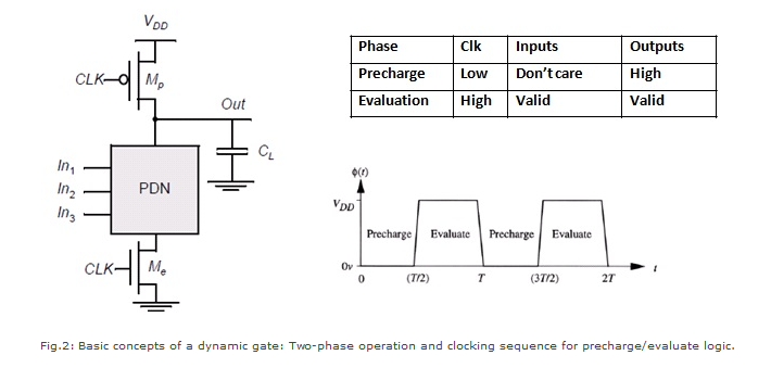
- Clamp Circuit Using Pmos And Nmos Devices Diagram Schematic And Image 07
- Tina Spice Tina Ti Import Pmos Problem Simulation Hardware System Design Tools Forum Simulation Hardware System Design Tools Ti E2e Support Forums
- Pmos Multisim Live
Find, Read, And Discover Pmos Circuit Diagram, Such Us:
- Ep0793345a1 Pseudo Nmos Or Pmos Inverter Google Patents
- Vlsi Design Mos Inverter Tutorialspoint
- Pmos Nand Gate Youtube
- Pmos 1 1 Multisim Live
- Mosfet Output Characteristics
If you re searching for Valence Electrons Lewis Dot Structure you've come to the right place. We ve got 104 images about valence electrons lewis dot structure including pictures, pictures, photos, backgrounds, and much more. In such web page, we additionally provide number of graphics out there. Such as png, jpg, animated gifs, pic art, symbol, black and white, translucent, etc.

Ep0793345a1 Pseudo Nmos Or Pmos Inverter Google Patents Valence Electrons Lewis Dot Structure

Transmission Gate As A Cmos Bilateral Switch Valence Electrons Lewis Dot Structure
I V Characteristics Of Pmos Transistor Analog Cmos Design Electronics Tutorial Valence Electrons Lewis Dot Structure

Pmos Nand Gate Youtube Valence Electrons Lewis Dot Structure
Virtual Lab Valence Electrons Lewis Dot Structure

Planet Analog Low Power Ldo Design Techniques For Really Small Profile Applications Part 2 Valence Electrons Lewis Dot Structure
Https Encrypted Tbn0 Gstatic Com Images Q Tbn And9gct41pqmv5g48gtvzxrqpvottegkwohy2thxo9jdo63wj9ya8c2i Usqp Cau Valence Electrons Lewis Dot Structure
2 Valence Electrons Lewis Dot Structure

High Side Driver Design Using Pmos With Resistive Load Electronicsbeliever Valence Electrons Lewis Dot Structure

Pmos Nor Gate Youtube Valence Electrons Lewis Dot Structure
Valence Electrons Lewis Dot Structure, Chapter 4 Computer Science Courses
- Problems With Dc Analysis Of A Pmos Circuit Electrical Engineering Stack Exchange
- Analysis Of Mosfet As A Switch With Circuit Diagram
- Transistor Level Implementation Of Cmos Combinational Logic Circuits
Valence Electrons Lewis Dot Structure, 13 Example Another Pmos Circuit Analysis Pdf Example Another Pmos Circuit Analysis 1 6 Example Another Pmos Circuit Analysis Consider The Pmos Course Hero
- Chapter 4 Computer Science Courses
- Ep0793345a1 Pseudo Nmos Or Pmos Inverter Google Patents
- Transistor Level Implementation Of Cmos Combinational Logic Circuits
Valence Electrons Lewis Dot Structure, The Symbol Of A A Pmos Transistor And B An Nmos Transistor Download Scientific Diagram
- Transistor Level Implementation Of Cmos Combinational Logic Circuits
- Pmos Multisim Live
- Http Vlab Amrita Edu Index Php Sub 59 Brch 165 Sim 270 Cnt 1
More From Valence Electrons Lewis Dot Structure
- Complete Tree Diagram
- Excel To Visio Flowchart
- Vivo Y51l Schematic Diagram
- Magnoliaceae Floral Diagram
- Legend Of Symbols Used On Wiring Diagrams
Incoming Search Terms:
- Http Vlab Amrita Edu Index Php Sub 59 Brch 165 Sim 270 Cnt 1 Legend Of Symbols Used On Wiring Diagrams,
- Nand And Nor Gate Using Cmos Technology Vlsifacts Legend Of Symbols Used On Wiring Diagrams,
- Transistor Level Implementation Of Cmos Combinational Logic Circuits Legend Of Symbols Used On Wiring Diagrams,
- Cmos Switch Bachelor Of Science Mechanical Engineering Studocu Legend Of Symbols Used On Wiring Diagrams,
- Chapter 4 Computer Science Courses Legend Of Symbols Used On Wiring Diagrams,
- Solved The Nmos And Pmos Transistors In The Below Circuit Chegg Com Legend Of Symbols Used On Wiring Diagrams,